This project was meant to provide an objective through which to build understanding of DMA and SPI channels on the RP2040. For this project, I chained two DMA channels. One of those channels is triggered by a timer which is configured to overflow at a fixed given interval. This channel moves data from a sine table to the SPI transmit buffer. The SPI channel is configured to automatically transmit any new data which appears in its transmit buffer.
The other DMA channel is chained to the first. When the first DMA channel finishes traversing the sine table, it triggers the second channel. This channel writes to the control registers of the first DMA channel. In particular, it writes to the AL3_TRANS_COUNT_TRIG register associated with the other DMA channel. This control register sets the number of transactions that the first DMA channel should execute (the length of the sine table). Because it is a trigger register, writing any non-zero value to this register automatically triggers the DMA channel to start. So, these two channels ping-pong off one another. The first finishes and triggers the second, the second writes to the control/trigger register of the first. The consequence is a persistent sine wave output from the DAC, with no code executing.
I used an MCP4822 DAC to generate a sine wave of a given frequency. The Pico transmits data to the DAC using SPI. The resources for the project include the C SDK User Guide, the RP2040 Datasheet and Prof. Hunter's website.
/*
 * Parth Sarthi Sharma (pss242@cornell.edu)
 * Code based on examples from Raspberry Pi Foundation.
 * The code sets up two DMA channels. One sends samples to the DAC,
 * (data_chan), and the other writes to the data_chan DMA control
 * registers (ctrl_chan).
 * The control channel writes to the data channel, sending one period of
 * a sine wave thru the DAC. The control channel is chained to the data
 * channel, so it is re-triggered after the data channel is finished. The control
 * channel then rewrites and restarts the data channel, etc.
 * NOTE: in order to configure the data channel read addresses to
 * wrap properly, the DAC data buffer must be naturally aligned in memory.
 * The solution was to use the ((aligned())) attribute.
 */

#include <stdio.h> //The standard C library
#include "pico/stdlib.h" //Standard library for Pico
#include "hardware/dma.h" //The hardware DMA library
#include <math.h> //Standard math library
#include "hardware/spi.h" //The hardware SPI library
#include "pico/time.h" //The pico time library
#include "hardware/adc.h" //The hardware ADC library

#define SIZE 256 //The size of the sine table

int sinTable[SIZE]; //The sine table
unsigned short DACData[SIZE] __attribute__ ((aligned(2048))); //The DAC data table

#define DAC_config_chan_A 0b0011000000000000 //The DAC configuration bits

#define CS 17 //The chip-select pin
#define MOSI 19 //The MOSI pin
#define MISO 16 //The MISO pin
#define SCK 18 //The clock pin
#define SPI_PORT spi0 //The SPI port to be used

const uint32_t tranCount = SIZE; //The transaction count

static inline void dma_channel_set_timer0(uint32_t timerval){ //The function to change the timer value in the DMA channel
    dma_hw->timer[0] = timerval;
}


int main(){ //The program running on core 0
    stdio_init_all(); //Initialize all of the present standard stdio types that are linked into the binary

    adc_init(); //Initialise the ADC hardware
    adc_gpio_init(26); //Initialise the gpio for use as an ADC pin
    adc_select_input(0); //Select an ADC input. 0...3 are GPIOs 26...29 respectively

    spi_init(SPI_PORT, 20000000); //Initialise SPI instance with the given baud rate
    gpio_set_function(MOSI, GPIO_FUNC_SPI); //Select GPIO function on the pin
    gpio_set_function(MISO, GPIO_FUNC_SPI); //Select GPIO function on the pin
    gpio_set_function(SCK, GPIO_FUNC_SPI); //Select GPIO function on the pin
    gpio_set_function(CS, GPIO_FUNC_SPI); //Select GPIO function on the pin
    spi_set_format(SPI_PORT, 16, 0, 0, 0); //Configure SPI with number of bits in each transaction, SPI mode (0, 0) and SPI order

    int i; //The counter i
    for(i = 0; i < SIZE; i++){ //For the sine table size
        sinTable[i] = (int)(2047 * sin((float) i * 6.283 / (float) SIZE) + 2047); //Create the sine table
        DACData[i] = DAC_config_chan_A | (sinTable[i] & 0x0fff); //Create the DAC data by masking sine table
    }

    int dataChannel = dma_claim_unused_channel(true); //The data channel
    int controlChannel = dma_claim_unused_channel(true); //The control channel

    dma_channel_config c = dma_channel_get_default_config(controlChannel); //Get configurations for control channel
    channel_config_set_transfer_data_size(&c, DMA_SIZE_32); //Set control channel data transfer size to 32 bits
    channel_config_set_read_increment(&c, false); //Set control channel read increment to false
    channel_config_set_write_increment(&c, false); //Set control channel write increment to false

    dma_channel_configure(controlChannel, &c, &dma_hw->ch[dataChannel].al1_transfer_count_trig, &tranCount, 1, false); //Configure control channel to write to data channel's al1_transfer_count_trig register

    dma_channel_config c2 = dma_channel_get_default_config(dataChannel); //Get configurations for data channel
    channel_config_set_transfer_data_size(&c2, DMA_SIZE_16); //Set control channel data transfer size to 16 bits
    channel_config_set_read_increment(&c2, true); //Set control channel read increment to true
    channel_config_set_write_increment(&c2, false); //Set control channel write increment to false

    //(X / Y) * sys_clk, where X is the first 16 bytes and Y is the second
    //sys_clk is 125 MHz unless changed in code
    dma_channel_set_timer0(0x0017ffff); //Write 0x0017ffff to timer 0 so that it gives a rate of 43869 (44kHz approx.)

    channel_config_set_dreq(&c2, 0x3b); //Select a transfer request signal. 0x3b means timer0
    channel_config_set_chain_to(&c2, controlChannel); //When this channel completes, it will trigger the channel indicated by chain_to
    channel_config_set_ring(&c2, false, 9); //Set address wrapping parameters

    dma_channel_configure(dataChannel, &c2, &spi_get_hw(SPI_PORT)->dr, DACData, SIZE, false); //Configure data channel to write to SPI port's dr register

    dma_start_channel_mask(1u << controlChannel); //Start control channel

    while(1){ //While eternity
        int adcIn = adc_read(); //Read the ADC value
        int timerVal = (((int) (adcIn / 7.45064)) << 16) + 65535; //Get the timer value by calculating X, left shifting it by 16 bits and adding 0xFFFF
        dma_channel_set_timer0(timerVal); //Change the timer value
    }
}
The first lines of code in the C source file include some header files. One of these is standard C headers (stdio.h) and the standard math header(math.h). The others are headers which come from the C SDK for the Raspberry Pi Pico. The first of these, pico/stdlib.h is what the SDK calls a "High-Level API." These high-level API's "provide higher level functionality that isn’t hardware related or provides a richer set of functionality above the basic hardware interfaces." The architecture of this SDK is described at length in the SDK manual. All libraries within the SDK are INTERFACE libraries.
The next includes pull in hardware APIs which are not already brought in by pico/stdlib.h. These include hardware/gpio.h, hardware/adc.h, hardware/irq.h, hardware/spi.h, pico/time.h and hardware/dma.h. As the names suggest, these interface libraries give us access to the API's associated with the hardware GPIO, hardware adc, hardware irq, hardware spi, pico time and hardware dma on the RP2040.
Don't forget to link these in the CMakeLists.txt file!
#include <stdio.h>
#include <math.h>
#include "pico/stdlib.h"
#include "hardware/gpio.h"
#include "hardware/adc.h"
#include "pico/time.h"
#include "hardware/irq.h"
#include "hardware/spi.h"
#include "hardware/dma.h"
The next section of the code is the #define's and the global variables which will be used throughout the code.
The following are the #define's to be used throughout the code:
The following are the variables to be used throughout the code:
Note: I have aligned the DACData array in memory. The reason for this will become obvious later in the code, but this is so that I can use the channel_config_set_ring option for the DMA channel, so that it will wrap its read address at the end of the array and start reading again at the beginning. For this to work, I need a naturally aligned array.
#define CS 17
#define MOSI 19
#define MISO 16
#define SCK 18
#define SPI_PORT spi0

#define SIZE 256

#define DAC_config_chan_A 0b0011000000000000

int sinTable[SIZE];
unsigned short DACData[SIZE] __attribute__ ((aligned(2048)));

const uint32_t tranCount = SIZE;
The SDK function channel_config_set_dreq(dma_channel_config *c, uint dreq) allows the programmer to select a transfer request signal for a particular DMA channel. The first argument is a pointer to channel configuration data, and the second is the dreq source. Sources for TREQ signals are internal (TIMERS) or external (DREQ, a Data Request from the system). 0x0 to 0x3a → select DREQ n as TREQ 0x3b → Select Timer 0 as TREQ 0x3c → Select Timer 1 as TREQ 0x3d → Select Timer 2 as TREQ (Optional) 0x3e → Select Timer 3 as TREQ (Optional) 0x3f → Permanent request, for unpaced transfers.
At present, there is no SDK function for manipulating the TIMER0, TIMER1, TIMER2, or TIMER3 registers. However, these registers are mapped to the dma_hw_t struct. The struct which organizes the DMA control registers is shown below:
typedef struct {
    dma_channel_hw_t ch[NUM_DMA_CHANNELS];
    uint32_t _pad0[16 * (16 - NUM_DMA_CHANNELS)];
    io_ro_32 intr;
    io_rw_32 inte0;
    io_rw_32 intf0;
    io_rw_32 ints0;
    uint32_t _pad1[1];
    io_rw_32 inte1;
    io_rw_32 intf1;
    io_rw_32 ints1;
    io_rw_32 timer[4];
    io_wo_32 multi_channel_trigger;
    io_rw_32 sniff_ctrl;
    io_rw_32 sniff_data;
    uint32_t _pad2[1];
    io_ro_32 fifo_levels;
    io_wo_32 abort;
} dma_hw_t;
We can manipulate each of the TIMER registers by touching the timer[4] array in this struct. The function dma_channel_set_timer0() modifies TIMER0 in particular. So, I'll configure the transfer request signal for the DMA channel to be TIMER0 by setting the dreq source to 0x3b.
Pacing (X / Y) Fractional Timer: The pacing timer produces TREQ assertions at a rate set by ((X / Y) * sys_clk). This equation is evaluated every sys_clk cycles and therefore can only generate TREQs at a rate of 1 per sys_clk (i.e. permanent TREQ) or less.
Note: By default, the sys_clk for the RP2040 is 125 MHz.
static inline void dma_channel_set_timer0(uint32_t timerval){
    dma_hw->timer[0] = timerval;
}
stdio_init_all();
In order to use the ADC, I first initialised the ADC using the adc_init() function. I then initialized the GPIO 26 using the adc_gpio_init() function. From the datasheet, I know that the ADC inputs 0 to 3 are connected to GPIOs 26 to 29 respectively. In order to select the input, I used the adc_select_input() function.
adc_init();
adc_gpio_init(26);
adc_select_input(0);
In order to initialise SPI instance, I used the spi_init() which takes in the SPI port and the baud rate as arguments. Then I used the gpio_set_function() to initialize the SPI pins with their respective functions. Lastly, I used the spi_set_format() function to configure how the SPI serialises and deserialises data on the wire.
spi_init(SPI_PORT, 20000000);
gpio_set_function(MOSI, GPIO_FUNC_SPI);
gpio_set_function(MISO, GPIO_FUNC_SPI);
gpio_set_function(SCK, GPIO_FUNC_SPI);
gpio_set_function(CS, GPIO_FUNC_SPI);
spi_set_format(SPI_PORT, 16, 0, 0, 0);
Initialize a 256 element wide sine table in order to contain the amplitudes for a single period of a sine wave. Next, I used the sine table values and masked them to form a DAC data table which can be directly sent to the SPI transmit buffer.
int i;
for(i = 0; i < SIZE; i++){
    sinTable[i] = (int)(2047 * sin((float) i * 6.283 / (float) SIZE) + 2047);
    DACData[i] = DAC_config_chan_A | (sinTable[i] & 0x0fff);
}
I claimed two DMA channels by making calls to the dma_claim_unused_channel() function. By making the argument to this call true, the function will panic if no DMA channels are available. Each call will return the name of a channel (an int) which we store in dataChannel and controlChannel, respectively.
int dataChannel = dma_claim_unused_channel(true);
int controlChannel = dma_claim_unused_channel(true);
I declared an object of type dma_channel_config and name that object c. This object is a struct and, initially, the fields of that struct are populated with those provided by the call to dma_channel_get_default_config(controlChannel). This function is as below:
/*! \brief  Get the default channel configuration for a given channel
 *  \ingroup channel_config
 *
 * Setting | Default
 * --------|--------
 * Read Increment | true
 * Write Increment | false
 * DReq | DREQ_FORCE
 * Chain to | self
 * Data size | DMA_SIZE_32
 * Ring | write=false, size=0 (i.e. off)
 * Byte Swap | false
 * Quiet IRQs | false
 * Channel Enable | true
 * Sniff Enable | false
 *
 * \param channel DMA channel
 * \return the default configuration which can then be modified.
 */
static inline dma_channel_config dma_channel_get_default_config(uint channel) {
    dma_channel_config c = {0};
    channel_config_set_read_increment(&c, true);
    channel_config_set_write_increment(&c, false);
    channel_config_set_dreq(&c, DREQ_FORCE);
    channel_config_set_chain_to(&c, channel);
    channel_config_set_transfer_data_size(&c, DMA_SIZE_32);
    channel_config_set_ring(&c, false, 0);
    channel_config_set_bswap(&c, false);
    channel_config_set_irq_quiet(&c, false);
    channel_config_set_enable(&c, true);
    channel_config_set_sniff_enable(&c, false);
    return c;
}
In the remainder of this code chunk, I made calls to a series of SDK functions to change some of these default channel configurations. Not all of these are strictly necessary (since they configure the channel to default settings), but are included for clarity. In particular, I set the transfer data size to 32 bits and turn off read/write incrementing.
dma_channel_config c = dma_channel_get_default_config(controlChannel);
channel_config_set_transfer_data_size(&c, DMA_SIZE_32);
channel_config_set_read_increment(&c, false);
channel_config_set_write_increment(&c, false);

dma_channel_configure(controlChannel, &c, &dma_hw->ch[dataChannel].al1_transfer_count_trig, &tranCount, 1, false);
Similarly to before, I declared an object of type dma_channel_config and name this one c2. I started with the default configurations, and then changed some of these configurations with subsequent calls to various channel_config functions from the SDK.
channel_config_set_dreq 0x3b.channel_config_set_chain_to(&c2, ctrl_chan);, the control dma channel will start automatically when the data channel finishes.channel_config_set_ring(&c2, false, 9);. The first argument is a pointer to the dma config structure c2. The second argument being false means that I am configuring read addresses (true here would instead configure a wrap boundary for write addresses). And finally, I specifed a 1 << 9 byte boundary on the read pointer. This means that the read address wraps on a (512-byte) boundary, so that the data channel reads the same array from beginning to end when it is next triggered. Why 512 bytes? The sine table is 256 elements long, each element is a 16-bit short, which is 2 bytes.Next, I started the control DMA channel. This will write to a triggered control register of the data channel, starting the first transfer of the the sine table out to the DAC. When the data channel completes, it triggers the control channel again (because I've chained the two). This starts the process over, and the two DMA channels ping-pong off of one another indefinitely.
dma_channel_config c2 = dma_channel_get_default_config(dataChannel);
channel_config_set_transfer_data_size(&c2, DMA_SIZE_16);
channel_config_set_read_increment(&c2, true);
channel_config_set_write_increment(&c2, false);

dma_channel_set_timer0(0x0017ffff);

channel_config_set_dreq(&c2, 0x3b);
channel_config_set_chain_to(&c2, controlChannel);
channel_config_set_ring(&c2, false, 9);

dma_channel_configure(dataChannel, &c2, &spi_get_hw(SPI_PORT)->dr, DACData, SIZE, false);
dma_start_channel_mask(1u << controlChannel);
For this code, the infinite while loop reads the ADC value and calculates the timer value for it. As we have established previously, the first 16 bits of the value represent X and the last 16 bits of the value represent Y. Therefore, I used the following algorithm to calculate the timer value:
int adcIn = adc_read();
int timerVal = (((int) (adcIn / 7.45064)) << 16) + 65535;
dma_channel_set_timer0(timerVal);
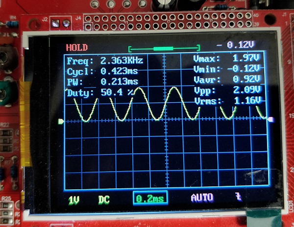
In order to view the output of the DAC, I used an oscilloscope. As it is quite evident from the oscilloscope output, the output of the DAC is a sine wave of the desired frequency.
cmake_minimum_required(VERSION 3.13)

include(pico_sdk_import.cmake)

project(SPIWithDMA)

pico_sdk_init()

add_executable(SPIWithDMA SPIWithDMA.c)

pico_enable_stdio_usb(SPIWithDMA 1)
pico_enable_stdio_uart(SPIWithDMA 1)

pico_add_extra_outputs(SPIWithDMA)

target_link_libraries(SPIWithDMA pico_stdlib hardware_dma hardware_spi hardware_adc pico_time)